This is an old revision of the document!
PCB with CNC
fritzing
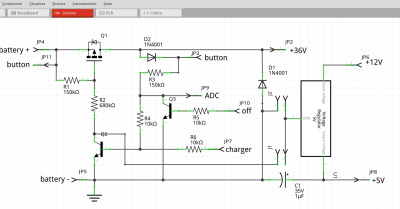
Make electronic schema with fritzing
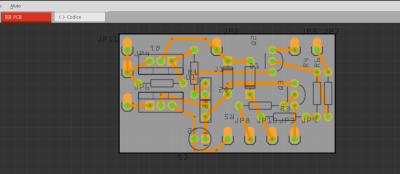
Make pcb routing:
- routing → DRC settings → 32mil large
- routing → DRC (check design at the end)
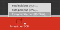
export gerber files
convert gerber to svg
Upload <name>_copperBottom.gbl to https://tracespace.io, select layers, download zip and extract <name>_copperBottom.gbl
Now with inkscape we need to process the complex SVG with multiples path, objects, layers, group, etc. to convert it into a single path simple SVG. You need to open your SVG into Inkscape (Open-Source, cross-platform), and perform the following series of commands:
- CTRL+A (Select all),
- CTRL+U (Ungroup),
- CTRL+ALT+C (Convert stroke to path),
- CTRL+A (Select all),
- CTRL+U (Union) and
- CTRL+SHIFT+R (Fit page to content).
- CTRL+S save
svg to gcode
Open jscut:
- load SVG <name>_copperBottom.gbl
- make all mm (link)
- zero lower left (link)
- select all objets, drills and path
- create operation
- outside, 0.1mm
- generate
- save gcode
edit gcode to set splindle speed to 8000 rpm and turn on it clockwise (after G90)
; after first G1
M3 S10000
carbide3d
set splindle speed to 8000 rpm and turn on it clockwise (after G90)
G00 Z1.000
M3 S10000
substitute G01 F400 with G01 F40
substiture G00 Z3.000 with G00 Z1.000
deprecated
- export your PCB as .svg files by clicking on “Export for PCB” on the bottom. Click on the small arrow on the Export button and select “Etchable (SVG)”. You will get a bunch of svg's exported in your selected directory but we will only use two of them:
- yourfilename*_etch_copper_bottom_mirror.svg
- yourfilename*_etch_mask_bottom_mirror.svg


